TSMC Confirms Wafer-Level Packaging Superior to Panel for Future AI Processors
TSMC has indicated that wafer-level packaging technologies, such as CoWoS, remain significantly more advanced than panel-level packaging for large AI processors. Kevin Zhang of TSMC stated that panel packaging is not expected to replace CoWoS in the near future for these demanding applications. The company is actively exploring panel-level packaging and developing its CoPoS technology, while wafer-level solutions are reportedly capable of scaling to incorporate 58 massive dies in a single package.
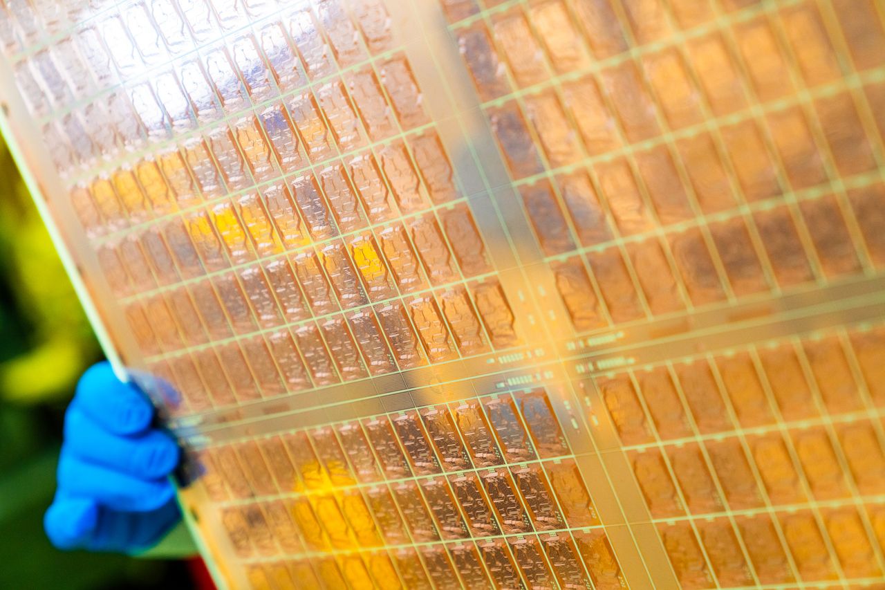
Taiwan Semiconductor Manufacturing Company (TSMC) has asserted that wafer-level packaging technologies currently hold a significant advantage over panel-level packaging, particularly for the largest artificial intelligence (AI) processors anticipated in the future.
Kevin Zhang, a representative from TSMC, commented that panel packaging is not expected to replace CoWoS (Chip-on-Wafer-on-Substrate) technology anytime soon. He highlighted that wafer-level packaging techniques are considerably more advanced than their panel-level counterparts.
Despite this assessment, TSMC is actively exploring panel-level packaging solutions and is engaged in the development of its own CoPoS (Chip-on-Package-on-Substrate) technology. The company also noted that current wafer-level technology demonstrates the capability to scale, allowing for the integration of up to 58 massive dies within a single package, addressing the growing demands of high-performance computing.
According to Tom's Hardware, this perspective underscores the ongoing advancements and strategic direction within semiconductor packaging technologies.